Research

We explore and control quantum spin systems at the ultimate size limit — single atoms, molecules and defects on surfaces — by combining electron spin resonance (ESR) with scanning probe microscopy. Our work runs along three connected lines: the physics of individual spins, the prototyping of molecular quantum units, and the instruments that make both possible.

Research area 01

Single Spin Resonance

A single spin is the smallest possible magnet — and, in principle, the smallest possible quantum bit and magnetic-field sensor. We use it as all three.

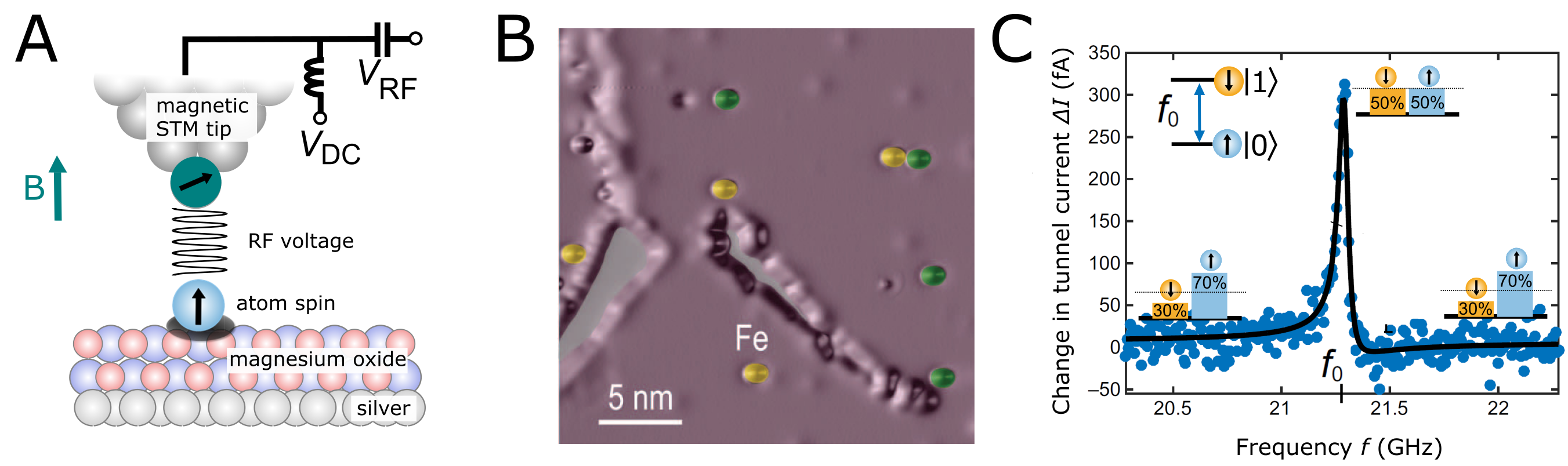
Schematic of single-atom electron spin resonance in an STM and an ESR spectrum
Magnetic atoms sit on bilayer MgO on a silver crystal; a radiofrequency voltage VRF added to the junction drives the Zeeman-split spin, and the resonance appears as a change ΔI in the spin-polarized tunnel current.

ESR in the scanning tunneling microscope

A magnetic atom is placed on a thin insulating film of magnesium oxide (MgO) and imaged by STM at low temperature in ultra-high vacuum. The MgO decouples the atomic spin from the conduction electrons of the silver substrate underneath, protecting its magnetic properties.

An external magnetic field Zeeman-splits the spin states |0⟩ and |1⟩; a radiofrequency voltage applied to the junction then drives the spin coherently, and the change in state population is read out through a spin-polarized tip acting as an atomic-scale spin filter. The scheme, first demonstrated in 2015 [Baumann et al., Science 350 (2015)], exceeds the energy resolution of conventional STM spectroscopy by roughly three orders of magnitude, reaching ~10 neV [Willke et al., Sci. Adv. 4 (2018)].
A single atom used as a quantum sensor, with dipolar splitting of its ESR line
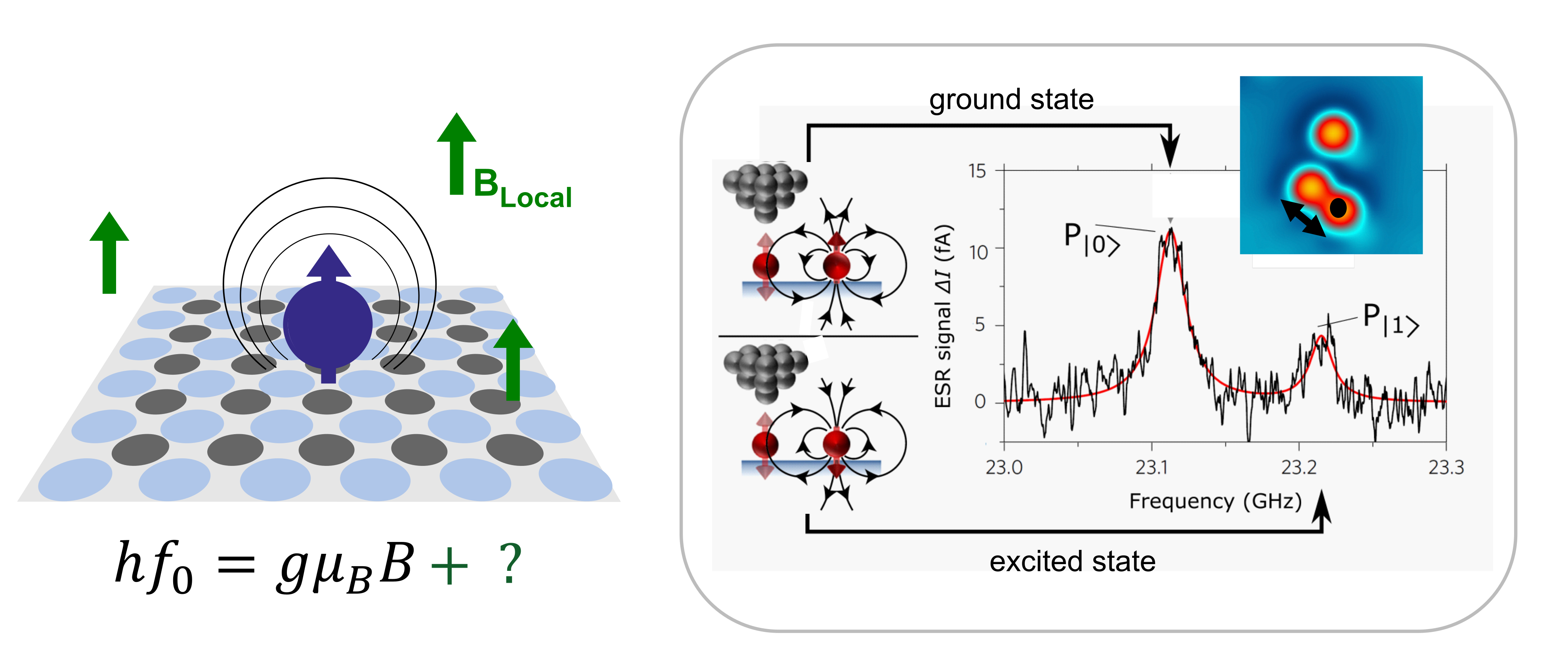
A single Fe atom as a quantum sensor: the dipolar field of a nearby target atom splits the sensor's ESR line by Δf, encoding the target's spin state and magnetic moment.

Quantum sensing with a single atom

The resonance frequency of an atom responds to any local magnetic field, so one atom can sense the magnetic environment around it. The combination of energy and spatial resolution makes the weak dipolar coupling between individual atoms measurable [Choi et al., Nat. Nanotechnol. 12 (2017)]: the ESR line of a sensor atom splits into two peaks that encode the spin state of a nearby target, and the splitting follows the r⁻³ law of dipolar interaction.

This determines magnetic moments to better than 0.01 μB and revealed spin lifetimes of several hours for single holmium atoms [Natterer et al., Nature 543 (2017)]. Below about one nanometre, exchange interaction takes over [Yang et al., PRL 119 (2017)].

Magnetic resonance imaging of a single atom
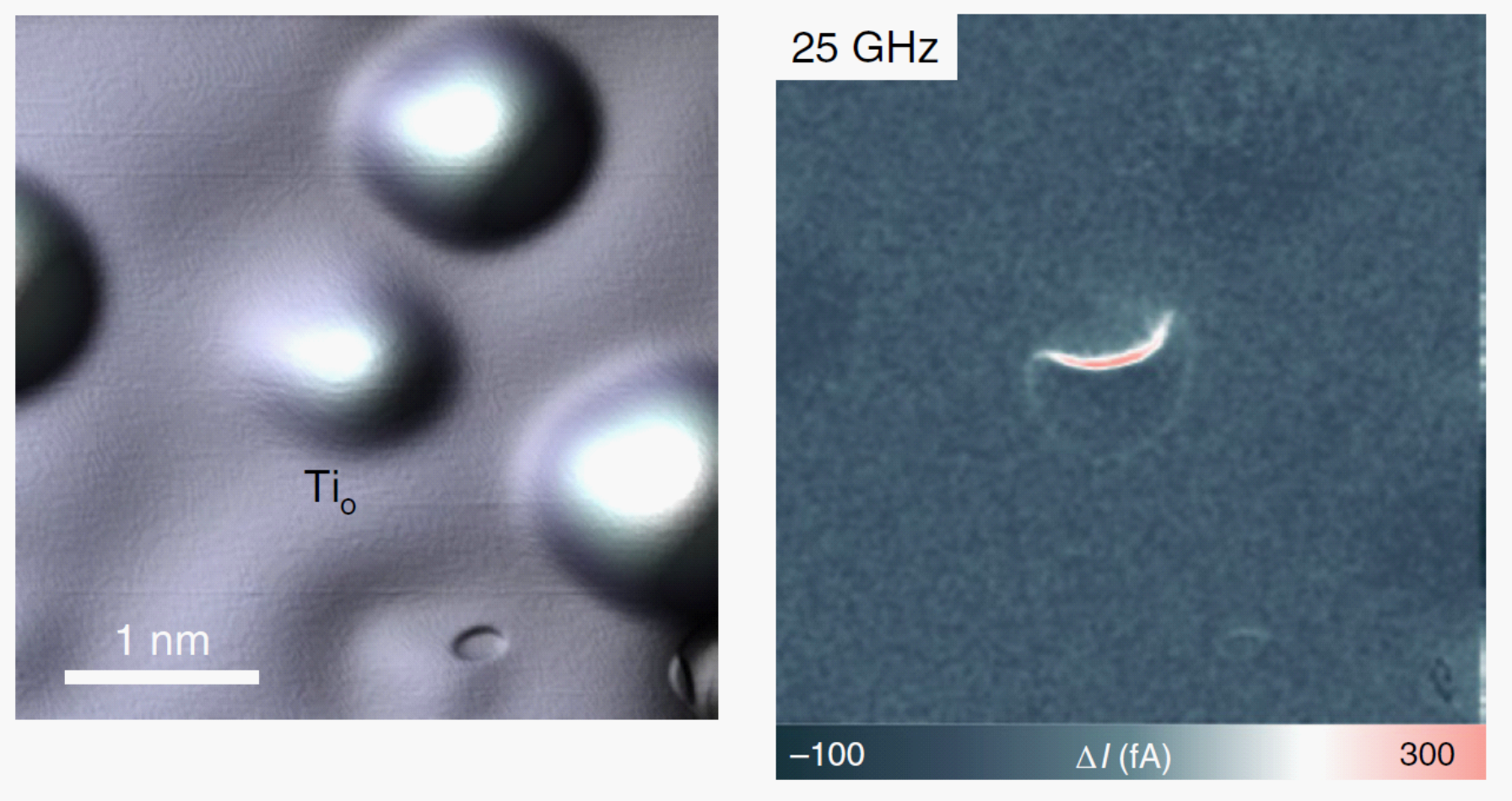
Atomic-scale MRI: STM topography of a single Ti atom (left) and the spatially resolved ESR signal (right), highlighting the resonant interaction with the magnetic tip.

Magnetic resonance imaging of single atoms

The magnetic tip interacts with the atomic spin as well, shifting the resonance with tip position. Turning that around — scanning the tip over the spin rather than placing a second atom next to it — establishes magnetic resonance imaging at the atomic scale [Willke et al., Nat. Phys. 15 (2019)].

The resulting maps resolve the three-dimensional magnetic interaction between surface spin and tip with a spatial resolution one to two orders of magnitude beyond other scanning-field-gradient techniques, and let the tip field itself be characterized and used as a controlled, local magnetic gradient [Willke et al., Nano Lett. 19 (2019)].

Hyperfine spectra of individual titanium isotopes and nuclear spin pumping in a copper atom
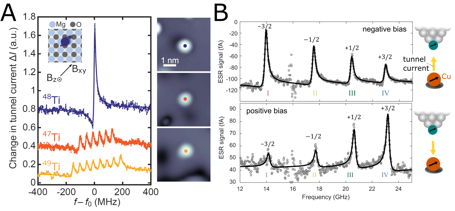
Hyperfine interaction of single atoms: distinct ESR multiplets for ⁴⁸Ti (I = 0), ⁴⁷Ti (I = 5/2) and ⁴⁹Ti (I = 7/2), and current-induced nuclear polarization of a single Cu atom.

Nuclear spins inside single atoms

The energy resolution reaches far enough to resolve the hyperfine coupling of an individual atom [Willke et al., Science 362 (2018)] — the first detection of single-atom nuclear spins in an STM, which makes isotopes distinguishable one atom at a time. Because the hyperfine splitting reflects the electronic ground state, its anisotropy reveals which orbital the unpaired electron occupies [Farinacci et al., Nano Lett. 22 (2022)], and moving an atom to a different binding site on MgO changes the spectrum accordingly.

The nuclear spin is not only observable but controllable: a spin-polarized tunnel current pumps it far from thermal equilibrium via spin-transfer torque [Yang et al., Nat. Nanotechnol. 13 (2018)], electron and nuclear spin exchange coherence within a single atom [Veldman et al., Nat. Commun. 15 (2024)], and the nuclear state can be read out in a single shot rather than as an ensemble average [Stolte et al., Nat. Commun. 16 (2025)] — the ingredients of a long-lived quantum memory attached to each atom.

Rabi oscillations and Hahn echo measurements on a single atom
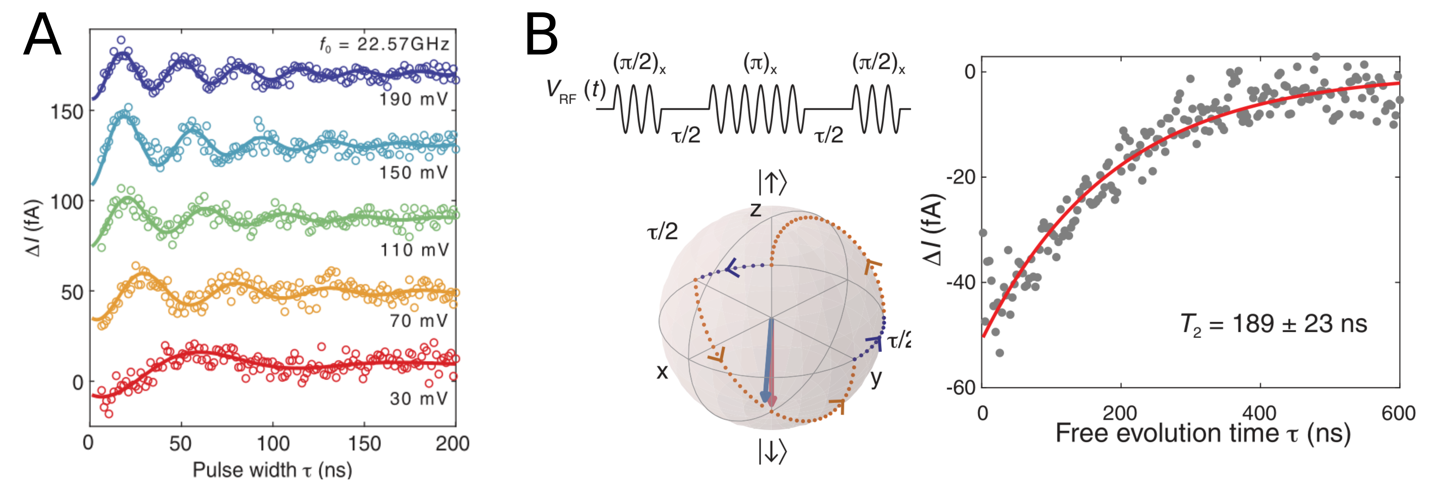
Coherent control: Rabi oscillations of a single Ti spin at different RF amplitudes, and a Hahn-echo sequence with the corresponding trajectory on the Bloch sphere.

Coherent control

With pulsed ESR the spin can be driven rather than merely detected: Rabi oscillations show controlled rotation of the state vector, and Hahn-echo sequences measure phase coherence times on the order of hundreds of nanoseconds [Yang et al., Science 366 (2019); Willke et al., Sci. Adv. 4 (2018)].
What limits them is the same tunneling current that provides the readout — and it also shapes how such an echo has to be read in the first place [Greule et al., New J. Phys. 28, 083501 (2026)]. Understanding — and eventually escaping — that trade-off between measurement and coherence is a running theme of our work.

Single spin defects in a two-dimensional semiconductor imaged by STM
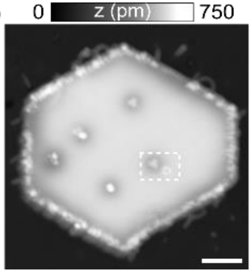
Atomic-scale quantum control of a single spin defect in a two-dimensional semiconductor.

Spin defects in two-dimensional semiconductors

Atoms on MgO are an almost ideal model system, but a technology needs spins that live inside a material. Point defects in two-dimensional semiconductors are a promising candidate: they are intrinsic to the host, they can be created and positioned during growth, and the surrounding lattice can be engineered.

We have extended atomic-scale quantum control to single spin defects in a 2D semiconductor, combining STM imaging of the individual defect with resonant driving of its spin [Au-Yeung et al., arXiv (2026)] — a route from single-atom model systems towards spin qubits embedded in a real solid-state host.

Key publications

Research area 02

Molecular Quantum Prototyping

Molecules are chemistry's answer to the qubit: identical by construction, tunable by design, and in principle manufacturable in bulk. We treat the microscope as an atomic workbench — assembling individual molecules into designed structures, addressing them electrically through the tunnel junction, and interrogating them with magnetic resonance. A candidate architecture can be built, driven, measured and discarded within a single experiment, long before anyone has to build a million of them.

A molecular double magnet and the Rabi map of its extended coherence
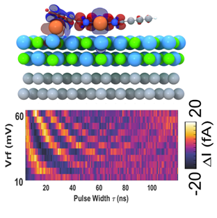
A molecular double magnet built from iron phthalocyanine and an additional iron atom, and the resulting Rabi oscillations as a function of drive amplitude and pulse width.

Building better molecular quantum units

The first question is what to build. Coupling a magnetic molecule to a second, deliberately chosen magnetic partner turns it into an on-surface molecular ferrimagnet whose level structure — and with it its coherence — is engineered rather than inherited: in double-magnet structures assembled from iron phthalocyanine and additional iron atoms, this extended the qubit lifetime severalfold [Huang et al., Nat. Commun. 16, 5208 (2025)].

Complementary spectroscopy of self-assembled organometallic complexes tells us how much magnetic moment survives contact with a surface [Huang et al., ACS Nano 19 (2025)], and how delocalized the molecular spin really is [Zhang et al., Nat. Chem. 14 (2022)].

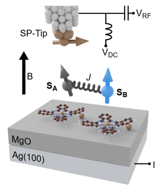
Two exchange-coupled molecules on MgO driven electrically through a spin-polarized tip
Two exchange-coupled molecular spins SA and SB on MgO/Ag(100): the exchange J turns the voltage at the junction into a handle on the molecular spin state.

Electrical initialization and control

A useful quantum unit must be set into a defined state and driven without a bulky field coil next to it. Through the exchange interaction with a nearby spin, an electric voltage becomes an effective handle on the molecular spin — spin–electric control that is faster and far more local than magnetic driving [Greule et al., Nat. Phys. (2026)]. Coherent driving of a molecular spin on a surface was established earlier in this way [Willke et al., ACS Nano 15 (2021)].

The same coupling lets a spin-polarized current pump the molecular spin out of equilibrium, giving electrical state initialization at the level of a single molecule [Greule et al., arXiv (2026)].

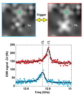
STM images and ESR spectra of a molecule switched between two magnetic configurations
A single-molecule spin switch: a voltage pulse toggles the molecule between two configurations, shifting its resonance between f₀A and f₀B.

Switches and the molecular environment

Beyond driving a fixed spin, molecules can change their magnetic state altogether. We demonstrated a single-molecule spin switch in which a voltage pulse toggles the molecule reversibly between two magnetic configurations — the molecular analogue of a bit that can be written and read [Huang et al., Nat. Commun. 16, 8242 (2025)].

The environment — neighbouring molecules, the substrate, the tip itself — is usually treated as what limits all of this, and mapping those interactions, from Kondo screening [Huang et al., ACS Nano 19 (2025)] to the exchange and dipolar coupling between assembled molecules [Zhang et al., Nat. Chem. 14 (2022)], tells us which molecular designs stand a chance outside the microscope.

But the same environment can be turned into an asset. A deliberately placed neighbouring spin — or a ferromagnetic electrode contacting the molecule — becomes a controlled knob rather than a nuisance, supplying the local exchange field that makes electrical driving and initialization possible in the first place [Greule et al., Nat. Phys. (2026)]. Designing the surroundings of a molecular qubit is therefore as much a part of the prototype as the molecule itself.

Key publications

Research area 03

Instrument Development

Every result above is limited by a machine. A large part of the group therefore builds the machines: colder, quieter, faster to turn around, and increasingly able to run themselves.

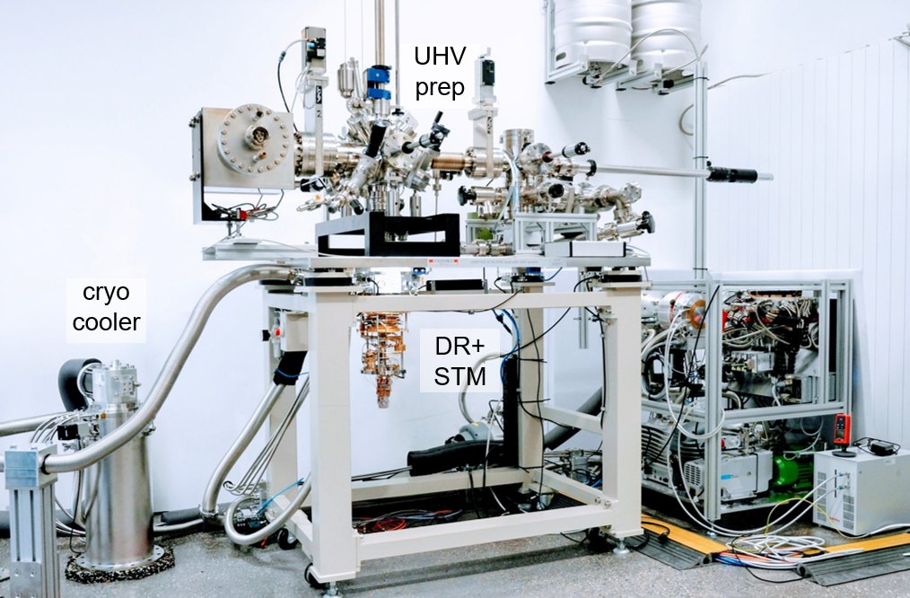
The quantum-ready ESR-STM: closed-cycle cryocooler, UHV preparation chamber and dilution-refrigerator STM

A quantum-ready ESR-STM

Coherent experiments need millikelvin temperatures, a magnetic field, microwave access to the junction and — above all — mechanical and thermal stability over days. Our instrument combines a dilution refrigerator and STM with an ultra-high-vacuum preparation stage, cooled by a closed-cycle cryocooler rather than liquid helium. That takes the cryogen supply out of the experiment entirely, holds conditions stable through long measurement runs, and allows fast warm-up and cool-down cycles, so changing a sample or a tip costs days instead of weeks — all in a deliberately compact design.

Developed together with the Wernsdorfer group at KIT and Qinu GmbH.

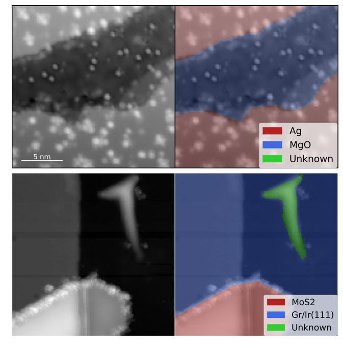
Neural-network segmentation of STM topographies into substrate, insulating film and unknown regions

A self-driving STM lab

A scanning probe experiment spends most of its time on work that is essential but not intellectually interesting: finding a clean area of surface, judging whether a tip is good enough, repeating a measurement until the statistics hold. We are automating that layer. Compact encoder–decoder neural networks, trained directly on raw topographic height data, segment an STM image into the regions that matter — bare substrate, insulating film, adsorbates, defects — accurately enough to steer the next measurement.

The models are deliberately small, on the order of tens of thousands of parameters, so a new material system can be taught in minutes on a single desktop GPU. Transfer learning makes it cheaper still: a network trained on one surface adapts to a completely different one from roughly a hundred labelled scans. The goal is a microscope that keeps doing useful work while nobody is watching it.

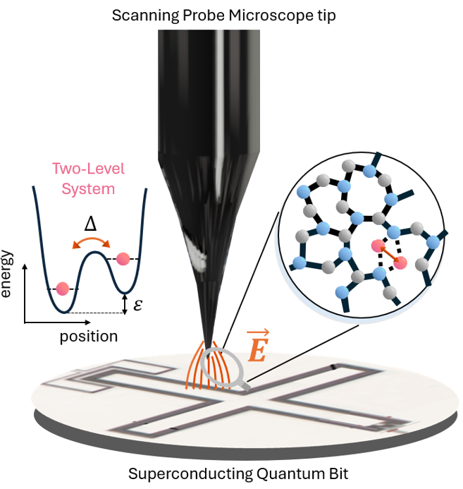
Scanning quantum defect microscope: a scanning probe tip above a superconducting qubit, sensing a two-level system

A scanning quantum defect microscope

Superconducting circuits are among the leading platforms for quantum computing, and their performance is degraded by quantum defects — in particular two-level systems (TLS) in the amorphous materials and interfaces of the device. Despite years of work their microscopic identity and spatial distribution remain largely unknown, because the qubit can only report that they are there, not where or what they are.

We are building an instrument to look at them directly: a scanning quantum defect microscope that combines atomic force microscopy with superconducting qubit spectroscopy, using the electric field beneath a scanning tip to tune and localize individual two-level systems on a working circuit. If it succeeds, the defects that limit superconducting qubits become visible objects instead of statistical nuisances.

A joint project with Hannes Rotzinger and Johannes Schwenk at KIT, funded 2026–2028 by the Volkswagen Foundation within Pioniervorhaben — Explorationen des unbekannten Unbekannten (Quantum Defects Made Visible).

Want to work on this?

These directions are funded through the ERC Starting Grant ATOMQUANT and further projects at KIT. See our publications for the latest results — and if any of it sounds like your kind of problem, come join us.